Isolated in 2004 by Andre Geim and Konstantin Novoselov, graphene is an exceptional nanomaterial, described as a "material of the 21st century" (European Graphene Flagship project with a budget of one billion euros over 10 years). Very light, impermeable, chemically inert, transparent, flexible yet extremely resistant and an excellent conductor of heat and electricity, its modular properties seem to open up multiple possibilities in almost all industrial sectors. The 16th session last February of the NanoRESP Forum was devoted to an overview of graphene and its technological, economic, health and social implications.
What are the properties of graphene? What applications have been tested? What is the position of France and Europe in this field? Have any risks of use been identified?
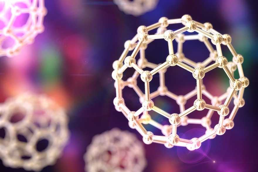
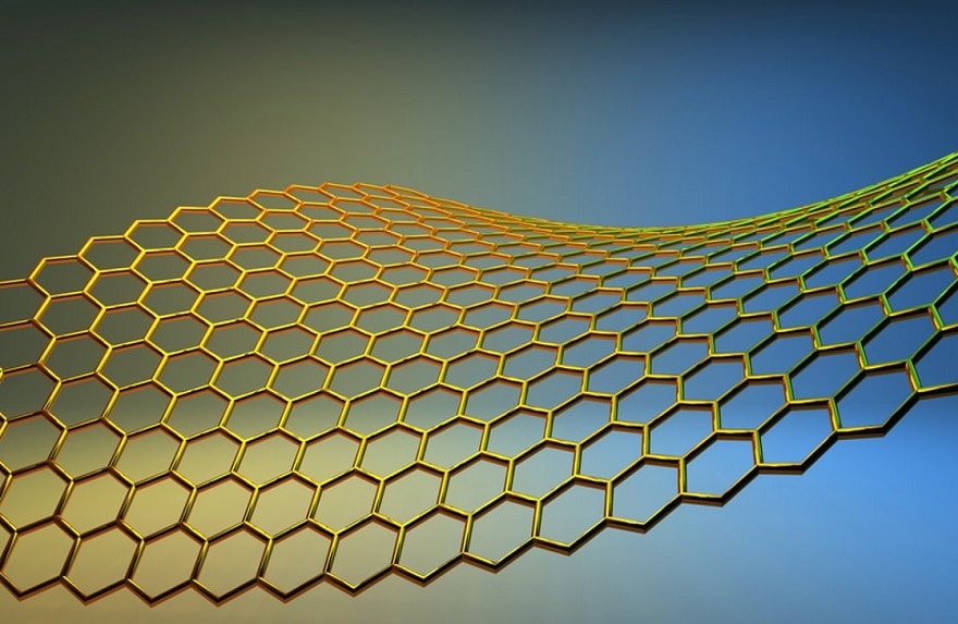
Ahe famous adhesive tape, scotch, has many virtues. Perhaps the least trivial, perhaps, is that it led to the discovery, in 2004, of a nanomaterial with exceptional properties, graphene. It is a nanomaterial consisting of a single plane of carbon atoms, a thickness of one tenth of a nanometre. It has been isolated from graphite, the constituent of pencil leads.

The latter consists of a stack of planes of carbon atoms organized at the vertices of a hexagonal network. These planes are linked by weak bonds called Van der Waals bonds, which makes the material brittle, exfoliable (it can be "peeled"). In 2004, two researchers from the University of Manchester, André Geim and Konstantin Novoselov, succeeded in exfoliating it for the first time. Their technique, which was extremely simple, involved... a tape! The tape tears off sheets of paper and transfers them to a silicon oxide substrate. Some of the fragments are monosheets, graphene. They can be identified under an optical microscope by their shades of grey, which is confirmed by atomic force microscopy. This exfoliation technique, combined with the measurement of the electrical properties of graphene, earned the two researchers the 2010 Nobel Prize in Physics (1).
The first 2D crystal
Graphene is thus the first two-dimensional crystal ever obtained," explains Annick Loiseau, a specialist in carbon nanomaterials at the Laboratoire d'étude des microstructures (LEM, UMR 104 Onera-CNRS) in Châtillon. Its mechanical, electronic, electrical, thermal and optical properties are exceptional. Without going into too much detail about physics, let's summarize them:
- Mechanical: in graphite, the carbon planes are weakly bonded together. In each graphene plane, on the other hand, the carbon atoms are linked by extremely strong bonds (they must be heated to very high temperatures to break them). As a result, the material is very mechanically resistant in the plane (100 times more than a steel of the same thickness), while being deformable. Combined with a shock absorbing material it can form very strong flexible materials.
- Electronic and electrical: the electrons moving in the plane are characterized by "Dirac cones", i.e. energies with behaviour similar to that of light. Their speed of movement is very high at room temperature, higher than that of conventional semiconductors, which ensures high electrical conductivity.
- Thermal: excellent thermal conductivity, 10 times better than copper, 20 times better than aluminium
- Optics: Graphene forms an ultra-transparent membrane (absorbing very few photons), which is suitable for the manufacture of flexible transparent electrodes.
New in recent years are materials that can be derived from graphene such as graphene oxide and graphane (each carbon atom is associated with a hydrogen atom). Graphene has above all brought the concept of heterostructures: graphene planes and other materials are combined to obtain new properties. Among the latter, boron nitride and the family of transition metal dichalkogenides (TMD) such as molybdenum disulphide (MoS2), tungsten disulphide (WS2), molybdenum diselenide (MoSe2) or tungsten diselenide (WSe2) are the most widely used for their electronic and optoelectronic properties. A whole field of discoveries has since been opened up, as the potential functional heterostructures are numerous.
What are they for? The fields of application are very numerous: filtering membranes, chemical and biological sensors, pressure sensors, composite materials, conductive inks, electronics (transistors, sensors), flexible and transparent devices (flexible screens, transparent conductors), photovoltaic energy, etc.

For this, graphene must be synthesized in industrial quantities. The technique of exfoliation by pulling off plans is not feasible at this scale. On the other hand, mass exfoliation of graphite is possible if the graphite is dispersed in a solvent ("liquid way"). The graphene sheets can then be separated using an energy source, such as ultrasound (sonication). The major way to obtain very good quality graphene with a large surface area (of the order of a square metre) is the Chemical Vapour Deposition (CVD) technique, which has long been used to obtain carbon tubes. At a temperature of 500 to 1,000°C, a hydrocarbon gas such as methane is decomposed on the surface of a catalytic metal substrate such as copper. The carbon resulting from the decomposition of the gas reorganizes to form graphene.
Another technique, called epitaxy or thermal graphitization, was developed in 2004 in parallel with mechanical exfoliation by Claire Berger and her colleagues (Walt de Heer's group at the Atlanta Institute of Technology). It uses a singular property of silicon carbide. This semiconductor, when heated to more than 1,000°C or under the pressure of an argon flux, becomes enriched with carbon on its surface: the silicon atoms evaporate (sublimation) while the carbon atoms rearrange themselves to form one or more graphene layers.
Depending on the synthesis processes used, graphenes of varying quality are obtained, more or less without defects, and for variable costs, the least expensive synthesis method being the exfoliation of graphite in solution while epitaxy is the most expensive. According to A. Loiseau, the whole game is to adapt the process according to what one wants to do with the graphene. For example, for an electricity conduction standard, medium quality graphene is sufficient. Integrated systems allowing both CVD synthesis and transfer of graphene to films have been developed in South Korea. In Europe, specialist companies are looking more to synthesize graphene and then transfer it by dry or wet transfer techniques to specific substrates which are then introduced into functional devices. The synthesis of heterostructures, which is more complicated, is not yet at the industrial stage but is the subject of intense research.
Multiple potential functions
Due to the arrangement of the carbon atoms in a single plane and the very large specific surface area thus created (2,630 m² per gram!), graphene can be surface modified by creating chemical bonds with various compounds. This functionalization makes it possible either to modify the properties of graphene, or to incorporate on the surface (i.e. adsorb) graphene active nanomaterials such as catalysts (to destroy pollutants, for example), proteins, drugs, fluorescent molecules, metallic nanoparticles, etc.
Probably the most useful functionalization at present, explained Stéphane Campidelli, from the Laboratory for Innovation in Surface Chemistry and Nanosciences (LICSEN), at CEA-Saclay, is the addition of oxygenated groups on the graphene planes of graphite. The graphite can then be exfoliated fairly easily to give graphene oxide sheets in suspension. This compound - which is insulating, unlike graphene - is much less expensive to obtain than graphene. The relative ease of exfoliation makes it possible to obtain larger surface area sheets than by direct exfoliation of graphite. The graphene oxide can then be deoxygenated (reduced) to give conductive graphene sheets with a large surface area.

Beyond oxygenation, a large number of chemical groups can be added, in theory, to graphene, using the main functionalization methods developed between 2000 and 2005 for carbon nanotubes. Two methods are used: covalent functionalization, through strong chemical bonds, or non-covalent functionalization, through weak interactions such as electrostatic forces. The first, also called chemisorption, has the advantage of producing stable and easy to handle assemblies, but the disadvantage (or advantage, depending on the purpose) of introducing irregularities in the carbon lattice, which alter its optical and electrical properties. The second, or "physisorption", is easier to achieve by depositing a solution containing the molecules of interest on graphene; it does not affect its electrical and optical properties but gives unstable assemblies; these are "supramolecular" assemblies. After several years of experimentation, chemists now have an arsenal of possibilities for "improving" graphene in the laboratory. On the other hand, the development of functionalization platforms for industrial purposes is still in its infancy.
Supercapacitors
Graphene seems to be most advanced in energy applications. Manufacturers are using it in particular in devices with a great future in electric vehicles, supercapacitors," explained Paolo Bondavalli, from the Thales Research and Technology Laboratory in Palaiseau. These devices have the advantage of having a high "power density", i.e. they can be charged and discharged in a few minutes without being exhausted, so that they can be charged and discharged up to a million times without any reduction in their capacity. On the other hand, they store much less energy than batteries (3 to 4 watt-hours per kg, compared to 30 to 40 Wh/kg for a battery). These "energy sprinter" characteristics - batteries being comparable to a marathon runner - have already led to their use in several fleets of buses or electric boats, in China to begin with but also in Europe (including Paris) more recently. These vehicles are recharged at bus stops, while passengers get on and off, each charge allowing them to travel several kilometres to the next stop. They can also be recharged while the vehicle is braking or, in the case of a cable car, when it is getting off. They are also used for operations requiring a rapid discharge of electrical power such as opening aircraft doors or lifting a forklift truck.
Technically, supercapacitors were invented by the Japanese company NEC in 1971. The term Electrical Double Layer Capacitor (EDLC) was coined. They consist of two metallic current collectors, carbon (activated carbon) electrodes impregnated with an electrolyte, and a separator that isolates the electrodes from each other. There are also hybrid capacitors in which materials added to the electrodes give an intermediate power density and energy density profile between those of supercapacitors and batteries. In addition to electric vehicles, one promising market for supercapacitors is mobile phone charging. One company, Zap and Go, has already marketed a graphene-based supercapacitor that charges in 5 minutes, which corresponds to a capacity of 2 kilowatts per kilogram of electrode material. Compared to the activated carbon used in the electrodes, graphene has the advantage of allowing more charge to pass through, i.e. its resistance is lower," explained Paolo Bondavalli. The Thales team is working on methods for synthesizing such composites in which carbon nanotubes are inserted between the graphene layers, which maintains the structure of the composite and improves its conductivity.
For example, a composite of 75 % graphene mixed with nanofibres increases electrical conductivity and power by a factor of 4 compared to activated carbon. The disadvantage of graphene is its preparation method in solution, which uses toxic solvents. To eliminate this disadvantage and to be able to switch to an industrial process, researchers are now opting for graphene oxide, which is less expensive and is very stable in water. Tests have shown that a proportion of 90 % of graphene oxide and 10 % of multiwall nanotubes optimizes charge storage. Such a composite, with a power density of 30 kilowatts per kilogram, would need 20 seconds to be recharged. All that remains is to move to industrial scale...
A biocompatible and biostimulating nanomaterial
Even more surprisingly, researchers have discovered since 2012 that graphene is biocompatible, meaning that cells are perfectly tolerant to its contact. What's more, explains Vincent Bouchiat, a physicist at the Néel Institute in Grenoble, experiments have shown that it stimulates the growth of living cells without altering their properties and functioning. We don't know why, but it could be because graphene has the same rigidity as the cells, so that they closely follow its surface. These discoveries have opened up new biomedical possibilities.
Vincent Bouchiat's team thus explored the extent to which a graphene monolayer obtained by vapour deposition, and then transferred to an insulating substrate, can serve as a platform for neuron growth. It showed that graphene, provided it is of very good quality, allows perfect adhesion of growing neurons to its surface and that the structure of adult neurons, after three weeks of culture, is better than that obtained on conventional biocompatible substrates such as glass coated with a layer of suitable proteins.
The interest is then to use the sensitivity to static and dynamic electrical charges of graphene to measure electrical cellular phenomena and to realize a bio-electronic interface more sensitive and more durable than with electronics based on more traditional materials such as metals or semiconductors.
Indeed, other experiments have shown that graphene field effect transistors (G-FETs) can detect the electrical activity of neurons, paving the way for new measuring devices. Biocompatible and biostimulant: two properties that have caught the imagination of researchers.
What if we use graphene to activate the healing process? Vincent Bouchiat has thus taken an interest in chronic wounds and ulcerations affecting, for example, diabetics and the elderly, sometimes leading to amputation. Within a spin-off of the Néel Institute, GRAPHEAL, he is currently testing the integration of graphene in a dressing that can be applied directly to wounds (2). Clinical trials are in progress. The long-term objective would be to take advantage of the electrical properties of graphene to create new-generation "intelligent dressings" capable of providing diagnostic data, for example relating to an infection, and to induce by electrostimulation a more rapid growth of the stem cells that heal the wound.

Does the biocompatibility of graphene mean that graphene poses no toxicity problems? Emmanuel Flahaut, from CIRIMAT in Toulouse (University of Toulouse, CNRS, INPT) (3) , in collaboration with Laury Gauthier's team (ECOLAB, Toulouse), reviewed this important but emerging question. Emmanuel Flahaut recalled the two justifications for studies on the health and environmental impact of carbon nanomaterials produced on an industrial scale, carbon nanotubes and graphene in particular: on the one hand, workers, including researchers, handle the raw particles; on the other hand, the particles end up in the environment and particularly in aquatic spaces through wear mechanisms of the materials, which end up accumulating all the pollutants.
The problem, which the NanoRESP forum has often mentioned, is that toxicity and ecotoxicity involve many parameters that are difficult to serialize: the dimensions of nanomaterials, their shape, their interaction surface (specific surface area in square meters per gram), their surface electric charge can be very variable, as well as the molecules adsorbed on them. From this point of view, there is not a graphene, but graphenes.
Globally, E. Flahaut (4) recalled, it is admitted that "the smaller it is, the more it transits", and that the larger the specific surface area, the greater the biological interactions. The publications on the toxicity of carbon nanoparticles highlight multiple disturbances on aquatic organisms such as the xenope, a widely used model amphibian, or the diatom Nitzschia palea. These organisms become contaminated by ingestion or by contact of their gills with nanoparticles suspended in water (5).
However, these results are quite far from the environmental reality as they are obtained with nanoparticle doses of several milligrams per litre, more than 1,000 times higher than their predicted potential concentrations in the environment.
Predictions of concentrations of carbon nanotubes made in Switzerland in particular by Bernd Nowak's group, based on the quantities produced and the exchange between media, lead to a concentration in surface waters of the order of 0.6 nanograms per liter at present. However, it can be expected to increase as industrial production increases.
A few points emerge from the studies carried out, summarises E. Flahaut: the more oxygen groups the material carries, the greater its impact. Graphene oxide is thus more toxic than pure graphene; it is particularly toxic for DNA (genotoxicity) whereas graphene is not, whatever its concentration. This is probably due to the greater chemical reactivity and easier dispersion in water of oxidized nanomaterials.
The second conclusion, based on the comparison of carbon nanomaterials, is that surface area is the best parameter for toxicity studies, while concentration (mass per litre) is hardly relevant. From this point of view, the large specific surface area of graphene sheets may be questionable, especially when it comes to graphene oxide. What will be done tomorrow with these impact studies? Can we not fear that they will weigh little in the balance in the face of the enormous potential of graphene illustrated in the course of this forum? We should probably start by increasing the number of impact studies at realistic concentrations of carbon nanomaterials. Can graphene and graphene oxide be eco-designed "safe(r) by design"? Researchers and working groups are talking about it, and scientific articles mention it (6) , but are there really the financial means to turn this slogan into reality in the various industrial fields concerned?
Conclusion
Unless one was a physicist, it was difficult to enter the quantum arcana of graphene to understand the origin of its unusual properties. However, everyone was able to perceive the enormous economic stakes involved, given the variety of current and potential applications of graphene. For example, supercapacitors are an astonishing energy mine. It remains to compare more precisely the advantages of graphene compared to other materials.
In passing, we have seen once again how basic research feeds into applied research. In the international concert, if we are to believe the European "flagship", France stands out for the timid commitment of its companies. Is it the context of the risks associated with nanomaterials that weighs on their strategies? The forum was not able to analyze it, but we can think that other, more structural and cultural factors are at play here.
Finally, as for all nanomaterials, the analysis of the risks related to the manufacture and use of graphene and its various forms seems to be organized without much effort, while "safe(r) by design" ecodesign is having difficulty making headway.
In a company that claims to be a risk manager, shouldn't this cross-cutting issue be integrated into the basis of any project?

The original of this article has been published on the website of the European Commission. NanoRESP - With our thanks to the authors.
(1 ) The Royal Swedish Academy of Sciences. "Scientific background on the Nobel Prize in physics 2010: Graphene", 5 October 2010. http://www.nobelprize.org/nobel_prizes/physics/laureates/2010/advanced-physicsprize2010.pdf
(2) https://www.linksium.fr/projet/grapheal/ http://www.grapheal.fr
(5) List of open access publications : https://oatao.univtoulouse.fr/view/people/Flahaut=3AEmmanuel=3A=3A.html
(6) For example, MVDZ Park et al, Considerations for Safe Innovation: The Case of Graphene, ACS Nano, 2017 Oct 24;11(10):9574-9593.
To go further :
- Book " La civilisation des nanoproduits " by Jean-Jacques Perrier - Edition Belin, September 2017
Anything to add? Say it as a comment.